We have moved to a new Website Check Now

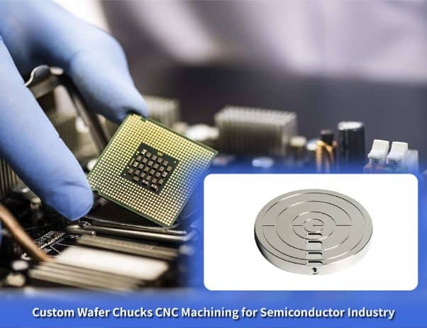
Custom Wafer Chucks CNC Machining for Semiconductor Industry

Custom wafer chucks are ultra-precision devices that hold and position silicon wafers in photolithography, inspection, etching, and deposition in semiconductor fabrication. Zintilon specializes in CNC machining custom wafer chucks, applying advanced techniques for grinding and lapping in order to attain exceptional flatness, temperature uniformity, and contamination control for defect-free wafer processing in cleanrooms.
  • Machining for complex chuck geometries and holding surfaces
  • Tight tolerances up to ±0.0001 in
  • Ultra-precision grinding, lapping & plasma-resistant finishing
  • Support for rapid prototyping and full-scale production
  • ISO 9001-certified semiconductor component manufacturing


Trusted by 15,000+ businesses

Why Semi-conductor Companies
Choose Zintilon

prductivity

Increased Productivity

Engineers get time back by not dealing with immature supply chains or lack of supply chain staffing in their company and get parts fast.

10x

10x Tighter Tolerances

Zintilon can machine parts with tolerances as tight as+/ - 0.0001 in -10x greater precision compared to other leading services.

world

World Class Quality

Zintilon provides aerospace parts for leading aerospace enterprises, verified to be compliant with ISO9001 quality standard by a certified registrar. Also, our network includes AS9100 certified manufacturing partners, as needed.

From Prototyping to Mass Production

Zintilon offers CNC machining for custom wafer chucks and for other holding fixtures to semiconductor equipment manufacturers, wafer processing tool suppliers, and semiconductor fabrication facilities worldwide.

Prototype Custom Wafer Chucks

Obtain high-precision prototypes of wafer chucks that replicate your final design. Test for flatness, vacuum hold, and contamination-free processing to guarantee performance prior to full-scale production.
Key Points:
Rapid prototyping with ultra-precision
Tight tolerances (±0.0001 in)
Test design, flatness, and thermal uniformity early
3 Axis CNC Machined Stainless Steel Passivation

EVT

Iterate quickly on wafer chuck protoype designs to meet all flatness and contamination standards. Spot issues early for easier scaling up to full semiconductor fabrication.
Key Points:
Validate prototype functionality
Rapid design iterations
Ensure readiness for production
Anodized Aluminum 1024x536

DVT

Validate design dimensional accuracy and thermal performance of custom wafer chucks with different materials to ensure design fidelity and process uniformity prior to mass production.
Key Points:
Confirm design integrity and flatness
Test multiple materials and surface treatments
Ensure production-ready performance
design aluminium

PVT

Assess custom wafer chucks for large-scale production and identify manufacturing challenges that may arise to ensure production efficiency prior to full-scale production.
Key Points:
Test large-scale production capability
Detect and fix process issues early
Ensure consistent part quality
Anodized Titanium Fastener

Mass Production

Rapid and precise production of contamination-free wafer chucks in cleanrooms with on-time delivery to semiconductor equipment manufacturers and wafer fabrication facilities, ensuring operational contamination-free.
Key Points:
Consistent, high-volume production
Ultra-precision machining for cleanroom quality
Fast turnaround with strict quality control
production

Simplified Sourcing for
the Semi-conductor Industry

Our aviation industry parts manufacturing capabilities have been verified by many listed companies. We provide a variety of manufacturing processes and surface treatments for aerospace parts including titanium alloys and aluminum alloys.

Explore Other Semiconductor Components

Browse our complete selection of CNC machined semiconductor components, crafted for durability and ultra-tight tolerances. From precision tooling and fixture parts to vacuum chambers and wafer handling systems, we deliver solutions tailored to advanced semiconductor production.

Materials for Custom Wafer Chucks

Custom Wafer Chucks CNC machining for the semiconductor industry is a product of our ultra-precision grinding and lapping facilities and our skilled semiconductor machining team. We engineer precision electrostatic chucks, vacuum chucks, and pin-type chucks for critical holding surfaces that ensure optimal wafer flatness, controlled temperatures, and particle-free processing during the various stages of wafer production. We specialize in ultra-precision surface grinding, lapping, and electrode integration, and design plasma-resistant coatings for wafer support and process compatibility as well as flatness control, measured with laser interferometry, and contamination control. For custom wafer chucks, we utilize ceramics (alumina, aluminum nitride), aluminum alloys (6061-T6), and composite materials that ensure semiconductor grade material compatibility and processing.
milling

CNC Machining

sheet metal

Sheet Metal Fabrication

edm

Wire EDM

Aerospace
Materials & Finishes

Materials
We provide a wide range of materials, including metals, plastics, and composites.
Finishes
We offer superior surface finishes that enhance part durability and aesthetics for applications requiring smooth or textured surfaces.

Specialist Industries

you are welcome to emphasize it in the drawings or communicate with the sales.

Materials for Custom Wafer Chucks

There is no shortage of materials available in our CNC machine shop for machining Custom Wafer Chucks for the semiconductor industry. To facilitate rapid prototyping and ultra-precision seam fabrication, we maintain contamination control and cleanroom compatibility with 10+ coatings of ceramics, metals, and composites.
Magnesium Image

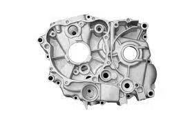
Due to the low mechanical strength of pure magnesium, magnesium alloys are mainly used. Magnesium alloy has low density but high strength and good rigidity. Good toughness and strong shock absorption. Low heat capacity, fast solidification speed, and good die-casting performance.

Price
$ $ $ $
Lead Time
< 7 days
Tolerances
Down to ±0.005 mm
Max part size
3000*2200*1100 mm
Min part size
2*2*2 mm
Steel Image

Steel is a strong, versatile, and durable alloy of iron and carbon. Steel is strong and durable. High tensile strength, corrosion resistance heat and fire resistance, easily molded and formed. Its applications range from construction materials and structural components to automotive and aerospace components.

Price
$ $ $ $ $
Lead Time
< 10 days
Tolerances
Down to ±0.001 mm (routing)
Max part size
3000*2200*1100 mm
Min part size
2*2*2 mm
Let’s Build Something Great, Together

FAQs: Custom Wafer Chucks for Semiconductor Applications

Custom wafer chucks are precision holding devices securing silicon wafers during semiconductor processing steps in fabrication equipment. There are electrostatic chucks (ESC) which use electrostatic force for chucking with embedded electrodes, vacuum chucks with porous ceramic or machined groove patterns providing suction holding, pin-type chucks which support wafers on minimal contact points thereby reducing backside contamination, thermal chucks which are capable of heating or cooling to 400°C or cryogenic temperatures, edge-ring supported chucks for plasma processes, proximity chucks for non-contact heating applications, and specialty chucks with multi-zone temperature control, embedded lift pins and edge exclusion designs, and plasma processes for wafers sizes 200mm, 300mm, and 450mm.

Aluminum nitride (AlN) has outstanding thermal conductivity of 170 watts per meter-Kelvin which allows for rapid equalization of the wafer temperature gradient to within 1°C across 300mm diameters making it easier to control the electrostatic chucking voltages to 2000V, and has high dielectric strength, and ultra-low particle generation, and near absolute plasma resistance to fluorine and chlorine chemistries. While alumina (Al₂O₃) has adequate thermal conductivity of 30 watts per meter-Kelvin, its superior mechanical strength, excellent plasma resistance, and lower cost relative to AlN, and proven reliability during etching and deposition processes make it a reasonable choice. Aluminum 6061-T6 has good thermal conductivity of 167 watts per meter-Kelvin, excellent machinability for complex cooling channels, cost-effectiveness for aluminum chucks, adequate vacuum compatibility with proper anodizing, and has adequate thermal conductivity for the cooling system. Composite materials are designed to synchronize the thermal expansion with the silicon wafer to prevent bowing. The coefficient of thermal expansion is 2.6 ppm per Kelvin.

For custom wafer chucks, ultra-precision surface grinding is utilized to achieve 0.0001 inches flatness at the wafer contact surface on a 300mm disk and a total thickness variation of less than 0.002 inches. For precision lapping, we develop surfaces with a micro finish of less than 0.1 microns Ra to contact wafers and to generate particles to contact surfaces. For our diamond grinding machines and diamond grinding for ceramic chucks, we design complex profiles. For CNC milling, we implement designs for the cooling channels, vacuum grooves, and mounting features. For coordinate `drilling, vacuum ports are produced and the lift pin holes drilled to a positional accuracy of ±0.003 inches, are drilled. Integrated are embedded electrodes for resistive heaters or electrostatic. For, vacuum grooves, we control the depth within ± 0.001 for a consistent holding force. Plasma spray coating provides yttria or alumina as a protective layer. All critical operations are performed in ISO Class 5 cleanrooms.

Options include anodizing on aluminum for the protection against corrosion, powder coating for environmental protection in custom colors where corrosion resistance exceeds 1000 hours in salt spray tests, zinc plating on steel for rust resistance, black oxide coating on steel for non-reflective surfaces in vision applications, bead blasting for uniform matte texture, and chromate conversion coating for electrical conductivity, while for precision grinding ultra-flat mounting surfaces are made with flatness made 0.003 inches.

Yes. We offer flexible manufacturing capabilities including:
Rapid prototyping for design validation
Low-volume production for specialized applications
High-volume production with consistent quality control
Full structural and dimensional verification at every stage
Got any more questions?